WLCSP and Wafer-Level Processing Services
We support your needs with our wide range of wafer-level processing technologies.
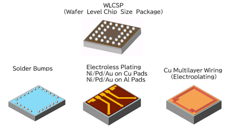
Service Lineup
| Package / Technology | Features | |
|---|---|---|
| WLCSP | Incorporates a thick, low-modulus polyimide layer to help relieve stress after board mounting. | |
| Helps reduce thermal and mechanical stress on the device. | ||
| Solder Bumps | Uses solder paste printing technology. | |
| Supports bump pitches down to 0.2 mm / 0.18 mm. | ||
| Electroless Plating | Cu-PAD | Forms Cu redistribution wiring over a polyimide layer on the device, followed by Ni/Pd/Au plating. |
| Enables wire bonding and stud bumping on the active surface of the IC. | ||
| Al-PAD | Ni/Pd/Au plating on Al pads enables Cu wire bonding. | |
| The robust Ni layer helps reduce stress transferred to the layers beneath the Al pad during wire bonding. | ||
Cu Multilayer |
Supports up to 7 layers: 4 dielectric resin layers and 3 metal layers. | |
| Minimum line/space: 10 μm / 8 μm. | ||
WLCSP and Wafer-Level Processing Line Overview
| Package / Technology | Features |
|---|---|
| Line Established | January 2004 (mass production started) |
| Supported Wafer Sizes | 6-inch and 8-inch |
| Major Equipment | Scrubber, Coater, Developer, Sputtering System, Exposure Tool, Cure Oven / Oven, Electrolytic Copper Plating System, Solder Printing Machine, Solder Ball Mounter, AVI |
Design Guide
Our design guide is available upon request.
Contact Us
For inquiries or requests regarding WLCSP and our wafer-level processing contract services, please contact us at the following: